https://www.freepatentsonline.com/y2022/0320042.html
the allocation of GPU processing pipeline components amongst multiple discrete dies to create smaller footprint building blocks (e.g., the various parallel processing stacked die chiplets described herein) that may be subsequently communicably stitched together with an active bridge chip enables manufacture of graphics pipes/chips scalable in a chiplet manner while still able to form a device having similar performance relative to a larger monolithic processor.
This modular 3D graphics concept is scalable, separately updatable, and mitigates the cost of assembly by using small die with high yield aspects, and provides value in not only allowing for increased die yield of production per semiconductor wafer but also increases the amount of good dies per semiconductor wafer.

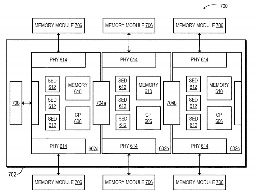
illustrated is a block diagram of a plan view 700 of a graphics processor MCM 702 employing graphics processing stacked die chiplets in accordance with some embodiments. The graphics processor MCM 702 (similar to the parallel processor MCM 202 of FIG. 2) is formed as a single semiconductor chip package including N=3 number of communicably coupled graphics processing stacked die chiplets 602 of FIG. 6. As shown in plan view 700, the graphics processor MCM 702 includes a first graphics processing stacked die chiplet 702a, a second graphics processing stacked die chiplet 702b, and a third graphics processing stacked die chiplet 702c.
As will be appreciated, the increased number of inter-die interconnect structures 608a,608b associated with graphics processing stacked die chiplets 602 allows for a larger number of stacked die chiplets to be communicably coupled together in a single package (e.g., relative to stacked die chiplets 402 which can only be paired, such as illustrated in FIG. 5, due to a single interconnect structure 408 on each stacked die chiplet 402). For example, in various embodiments, the graphics processor MCM 702 includes a first bridge chip 704a that communicably couples the first graphics processing stacked die chiplet 702a to the second graphics processing stacked die chiplet 702b. In particular, the first bridge chip 704a communicably couples the second inter-die interconnect structure 608b of the first graphics processing stacked die chiplet 702a to the first inter-die interconnect structure 608a of the second graphics processing stacked die chiplet 702b. Additionally, the graphics processor MCM 702 includes a second bridge chip 704b that communicably couples the second graphics processing stacked die chiplet 702b to the third graphics processing stacked die chiplet 702c. In particular, the second bridge chip 704b communicably couples the second inter-die interconnect structure 608b of the second graphics processing stacked die chiplet 702b to the first inter-die interconnect structure 608a of the third graphics processing stacked die chiplet 702c.
In various embodiments, the bridge chips 704 are passive or active, in which each bridge chip 704 includes just data/electrical connections or a given bridge chip 704 includes its own logic. For example, in some embodiments, each bridge chip 704 is an active bridge chip having active silicon to operate as a high-bandwidth die-to-die interconnect between the graphics processing stacked die chiplets 602. In other embodiments, the bridge chip 704 is a passive chip.
In some embodiments, an active bridge chip 704 includes one or more cache buffers and therefore extends beachfront edge connectivity, while still providing inter-base-die communications and to route cross die synchronization signals. Caches are naturally an active component (i.e., require electrical power for operations), so the bridge chip 704 is active for holding those cache buffers. Cache sizing is configurable, for example, as a function of the physical size of the active bridge chip 704, for different applications along with different stacked die chiplet configurations, and the stacked die chiplet(s) to which the active bridge chip 704 is communicably coupled do not pay the cost (e.g., costs related to physical space, power constraints, and the like) of this external cache on the bridge chip 704.
In various embodiments, the bridge chip 704 includes a local silicon interconnect (LSI) that provides a small silicon bond in free translation that communicably couples two logic chips together and provides inter-die connectivity between adjacent edges of the two dies with a limited physical scope (e.g., as opposed to mounting the stacked die chiplets 602 to a common interposer substrate and relying entirely on electrical connections provided by the interposer for inter-die communications, such as provided by conventional 2.5D topologies in which the interposer often spans the extent of an entire assembly). In this manner, the intermediary bridge chip 704 communicably couples multiple stacked die chiplets (e.g., the first graphics processing stacked die chiplet 602a and the second graphics processing stacked die chiplet 602b) together. Additionally, in various embodiments, the bridge chip 704 carries a data fabric (not shown) between the two stacked die chiplets to provide a common view of memory.
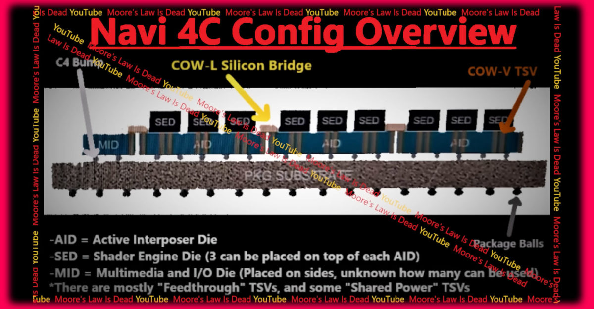
The coupling of multiple graphics processing stacked die chiplets (e.g., first graphics processing stacked die chiplet 602a to the second graphics processing stacked die chiplet 602b, which is in turn coupled to the third graphics processing stacked die chiplet 602c) together in a single package results in a device that effectively operates as a single large graphics complex die (GCD) but is constructed out of smaller, modular die components. In various embodiments, the graphics processor MCM 702 is communicably coupled to one or more external system memory modules 706 via the memory controller PHYs 614 of the graphics processing stacked die chiplets. Additionally, in some embodiments, the graphics processor MCM 702 also includes input/output (I/O) logic in a multimedia and I/O die (MID) 708 separate from the graphics processing stacked die chiplets 602.
![[H]ard|Forum](/styles/hardforum/xenforo/logo_dark.png)
