Yep, at least there is someone here with a good explaination. I have a 7800 GS and it has a PCI-e to AGP brdige chip on it. The 8800GTX wouldn't need one of those though, so it must be for physics.KompressorV12 said:unless something changed, in the leaked release documents it says the G80 will come with a PPU, I bet you that is the chip for it
Navigation
Install the app
How to install the app on iOS
Follow along with the video below to see how to install our site as a web app on your home screen.
Note: This feature may not be available in some browsers.
More options
You are using an out of date browser. It may not display this or other websites correctly.
You should upgrade or use an alternative browser.
You should upgrade or use an alternative browser.
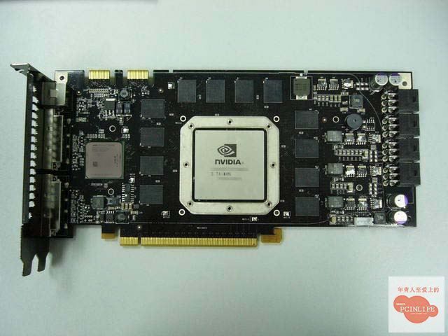
G80 naked with mystery chip
- Thread starter nobody_here
- Start date
w1retap
[H]F Junkie
- Joined
- Jul 17, 2006
- Messages
- 13,712
Yea, it must be. Nobody knows what it is except the people at Nvidia that worked on the thing. Speculation isn't truth.belmicah said:Yep, at least there is someone here with a good explaination. I have a 7800 GS and it has a PCI-e to AGP brdige chip on it. The 8800GTX wouldn't need one of those though, so it must be for physics.
revenant
[H]F Squad Captain
- Joined
- Apr 10, 2005
- Messages
- 16,311
(cf)Eclipse said:sli helper chip thingy")
this was my guess also. it's the "oh shit, SLI is b0rked" chip.
shadowlord
2[H]4U
- Joined
- Jan 6, 2005
- Messages
- 3,109
looks like a geforce 2 chip, so you could play all your vintage games on it to !!
too big for DRM/HDCP purposes, nvidias physics implementation will most likely be a separate PCI-E card. IMO it could be one of the following:
1) Onboard Physics
2) Some kind of compatability chip for DX9 or below games.
3) HD video Decoder/accelerator or something similar.
4) A switch/processor/bridge for the physics PCI-E card.
5) Embeded memory for AA/AF
1) Onboard Physics
2) Some kind of compatability chip for DX9 or below games.
3) HD video Decoder/accelerator or something similar.
4) A switch/processor/bridge for the physics PCI-E card.
5) Embeded memory for AA/AF
MrWizard6600
Supreme [H]ardness
- Joined
- Jan 15, 2006
- Messages
- 5,791
my GOD i have been looking for this picture for 2 MONTHS. and its HERE. and its SWEET.
but umm one question for OP, wtf is DRM?
edit: and i knew it was going to look funky, this explains the two pci-e connectors. two dies, two connectors, each of them just want some love.
edit2:
QFT
sooo excited now man. seen the boxed ver from asus, seen the board, now OCP its time for you to rip it apart and give me some specs
altho kyle said "overclocking the G80 is like a pale full of [something, cant remember exactly what he said... but it sounded good]" so.... so happy
but umm one question for OP, wtf is DRM?
edit: and i knew it was going to look funky, this explains the two pci-e connectors. two dies, two connectors, each of them just want some love.
edit2:
revenant said:this was my guess also. it's the "oh shit, SLI is b0rked" chip.
QFT
sooo excited now man. seen the boxed ver from asus, seen the board, now OCP its time for you to rip it apart and give me some specs
altho kyle said "overclocking the G80 is like a pale full of [something, cant remember exactly what he said... but it sounded good]" so.... so happy
digitalfreak
Limp Gawd
- Joined
- Apr 18, 2005
- Messages
- 356
No, it is a PCI-E -> AGP bridge chip, as there will be AGP versions of this card. Nvidia has heard the cries of all those folks refusing to leave the 20th century, and allowed them to run an 8800GTX on their Athlon T-bird systems. It also handles re-combining the video output from both cards in SLI, as Nvidia has decided to go with an external dongle solution.belmicah said:Yep, at least there is someone here with a good explaination. I have a 7800 GS and it has a PCI-e to AGP brdige chip on it. The 8800GTX wouldn't need one of those though, so it must be for physics.
revenant
[H]F Squad Captain
- Joined
- Apr 10, 2005
- Messages
- 16,311
^^that makes complete sense.. I bet that's it.
MrWizard6600 said:but umm one question for OP, wtf is DRM?
digital rights management
digitalfreak said:No, it is a PCI-E -> AGP bridge chip, as there will be AGP versions of this card. Nvidia has heard the cries of all those folks refusing to leave the 20th century, and allowed them to run an 8800GTX on their Athlon T-bird systems. It also handles re-combining the video output from both cards in SLI, as Nvidia has decided to go with an external dongle solution.
There will be no 8800GTS for AGP, since G80 is PCI-E native why the hell would they use a bridge chip on the PCI-E version of the card? AGP versions may well appear however they will not be 8800GTX/GTS's and definetly not now.
digitalfreak
Limp Gawd
- Joined
- Apr 18, 2005
- Messages
- 356
It's very similar to RTFM.MrWizard6600 said:but umm one question for OP, wtf is DRM?
MrWizard6600
Supreme [H]ardness
- Joined
- Jan 15, 2006
- Messages
- 5,791
thx brinox
edit: thx digitalfreak
edit: thx digitalfreak
w1retap
[H]F Junkie
- Joined
- Jul 17, 2006
- Messages
- 13,712
lol.. but why would it need a seperate chip for doing DX9 stuff.... Do our current boards need a whole dedicated chip the size of a US quarter to do DX7 stuff? I thought direct x was just software that used the new hardware capabilities to help render the graphics. (shader technologies, etc) If so, it would be backwards compatible easily since the chip would be powerful enough to compute everything the previous generations of cards could do.
ThreeDee said:The chip is there so you can run embedded Linux on your video card to handle the new DX10 functions .. nVidia calls it the 8800KILLERgtx ... they're still working on a "K" shaped passive cooler for it tho ... I just read that over at the INQ

omg i about died laughing when i read that... as its already been said, i think its something to do with embedded physics processing of some sort, why else would there be odd specs, like 512 + 256mb of video memory and a 256bit + 128bit memory interface. to me its obvious there is two separate computing systems on this card, one is a 512mb GPU with a 256bit memory interface and then an unknown 256mb + 128bit memory interface, which also doubles as additional horsepower for GPU stuff when needed.
my guess is that when nvidia releases some sort of physics solution these new cards will work with the additional 256mb + 128bit system.
w1retap
[H]F Junkie
- Joined
- Jul 17, 2006
- Messages
- 13,712
I'm thinking now it has something to do with the new dual rail SLI, or dual channel SLI.
digitalfreak
Limp Gawd
- Joined
- Apr 18, 2005
- Messages
- 356
It also enhances the size of your penis and makes you last longer in bed. Apparently you didn't get the joke...kleox64 said:There will be no 8800GTS for AGP, since G80 is PCI-E native why the hell would they use a bridge chip on the PCI-E version of the card? AGP versions may well appear however they will not be 8800GTX/GTS's and definetly not now.
revenant
[H]F Squad Captain
- Joined
- Apr 10, 2005
- Messages
- 16,311
8800V(ia)GRA
MrWizard6600
Supreme [H]ardness
- Joined
- Jan 15, 2006
- Messages
- 5,791
yeah thats what im thinking too. been looking alot recently at expected numbers, they all give the odd bus and the odd ram.
they also mention the seperate "geometry function", that was just a function of DX10, and on the integrated shader model.
maybe Nvs pushed the idea a little further, givin it its own bus and memory, and now makes it not only render the polygons, but smash em together too.
they also mention the seperate "geometry function", that was just a function of DX10, and on the integrated shader model.
maybe Nvs pushed the idea a little further, givin it its own bus and memory, and now makes it not only render the polygons, but smash em together too.
w1retap said:I'm thinking now it has something to do with the new dual rail SLI, or dual channel SLI.
You might be onto something there. Maybe SLI for dual or dual link monitors now? Compositor/hardware antialiasing chip anyone?
digitalfreak
Limp Gawd
- Joined
- Apr 18, 2005
- Messages
- 356
Nope. Octa-SLI.yevaud said:You might be onto something there. Maybe SLI for dual or dual link monitors now? Compositor/hardware antialiasing chip anyone?
MrWizard6600
Supreme [H]ardness
- Joined
- Jan 15, 2006
- Messages
- 5,791
...digitalfreak said:Nope. Octa-SLI.
four PCBs. design it just like the 7950GX2, only with two cores on each PCB
brinox said:digital rights management
Nvidia's calling it "Mediashield ®"
brinox said:omg i about died laughing when i read that... as its already been said, i think its something to do with embedded physics processing of some sort, why else would there be odd specs, like 512 + 256mb of video memory and a 256bit + 128bit memory interface. to me its obvious there is two separate computing systems on this card, one is a 512mb GPU with a 256bit memory interface and then an unknown 256mb + 128bit memory interface, which also doubles as additional horsepower for GPU stuff when needed.
my guess is that when nvidia releases some sort of physics solution these new cards will work with the additional 256mb + 128bit system.
the memory bandwidth has gone up by 50%, since thier using only slightly faster memory than the current 7900GTX, the higher memory bandwidth must be from the wider memory bus meaning it isnt separate.
MrWizard6600
Supreme [H]ardness
- Joined
- Jan 15, 2006
- Messages
- 5,791
kleox64 said:the memory bandwidth has gone up by 50%, since thier using only slightly faster memory than the current 7900GTX, the higher memory bandwidth must be from the wider memory bus meaning it isnt separate.
dont buy that, its just to weird a number.
revenant
[H]F Squad Captain
- Joined
- Apr 10, 2005
- Messages
- 16,311
SLI is on the main die.. I remember that... since the 7800 series on up.. but they also said SLI was not working well.. so it might have needed something.. well, I still think it's a pci-e --> agp bridge chip.. for the agp version.. notice it's only on the 8800GTS, the lesser version...which will be the only agp version..
or wait.. I didn't notice the 'keep out' thing before.. lol
8800GTX

8800GTS

or wait.. I didn't notice the 'keep out' thing before.. lol
8800GTX
8800GTS
MartinX said:The sli and media stuff is going to be on the main die, HDCP is the only external functionality we're going to see on these.
The 7950gt has HDCP support, but I don't recall seeing an extra chip...
w1retap
[H]F Junkie
- Joined
- Jul 17, 2006
- Messages
- 13,712
The second SLI connector is for dual rail SLI. "The Inquirer" just released another set of info about it. It can read/write at the same time or something. http://www.theinquirer.net/default.aspx?article=35318Dillusion said:christ thats a huge main die, is that an IHS on it?
Why the second SLI connector? bottleneck alredy?
w1retap
[H]F Junkie
- Joined
- Jul 17, 2006
- Messages
- 13,712
oh em eff gee. The new 8800GTO with the chip revealed. It appears to be an AMD FX-62. It needs a little more power too.. and dual SLI links.
revenant
[H]F Squad Captain
- Joined
- Apr 10, 2005
- Messages
- 16,311
^^ lol
full duplex data flow. what a concept. but that is good.. SLI performance should continue to be tuned and improved both in hardware and in software. Nice stuff.
EDIT: but the old function of the bridge was just to send the video data over to the frame buffer card for final assembly.. I didn't know there was a lot of need to write data back to the "slave" card - but oh well.. I guess having seperate data paths would be more optimal..
w1retap said:The second SLI connector is for dual rail SLI. "The Inquirer" just released another set of info about it. It can read/write at the same time or something. http://www.theinquirer.net/default.aspx?article=35318
full duplex data flow. what a concept.
but that is good.. SLI performance should continue to be tuned and improved both in hardware and in software. Nice stuff. EDIT: but the old function of the bridge was just to send the video data over to the frame buffer card for final assembly.. I didn't know there was a lot of need to write data back to the "slave" card - but oh well.. I guess having seperate data paths would be more optimal..
chinesepiratefood
2[H]4U
- Joined
- Oct 8, 2005
- Messages
- 2,629
maybe it is to make SLI-AA usable at >8x
LOCO LAPTOP
[H]F Junkie
- Joined
- May 4, 2006
- Messages
- 12,644
w1retap said:oh em eff gee. The new 8800GTO with the chip revealed. It appears to be an AMD FX-62. It needs a little more power too.. and dual SLI links.
haha nice photoshop
and the only question is "can you overclock it?" meatfestival
[H]ard|Gawd
- Joined
- Apr 5, 2005
- Messages
- 1,767
How do you get 640MB out of 12 RAM chips? (see 8800GTS). Perhaps 8x64 + 4x32?
And, according to another picture, the GTS will only have one SLI connector on the board, while the GTX will have 2.Battle_Rattle said:So the 8800GTS needs one power dongle while the higher end one needs two?
mastercheeze
2[H]4U
- Joined
- Jul 23, 2004
- Messages
- 2,799
Maybe the GTX is the only one with the physics chip, and the second bridge is for physics data? SLI QUANTUM PHYSICS
/rampant speculation
/rampant speculation
w1retap
[H]F Junkie
- Joined
- Jul 17, 2006
- Messages
- 13,712
512 normal video ram, 128 dedicated to special tasks like AA. ^_^meatfestival said:How do you get 640MB out of 12 RAM chips? (see 8800GTS). Perhaps 8x64 + 4x32?
Commander Suzdal
2[H]4U
- Joined
- Jul 29, 2004
- Messages
- 2,134
Man, the only reason I clicked on this thread was because I thought the title was, "G80 naked with mystery CHICK!!!" What a ripoff....